Coupled Simulation to Determine the Impact of Across Wafer Variations in Oxide PECVD on Electrical and Reliability Parameters of Through-Silicon Vias (TSVs)
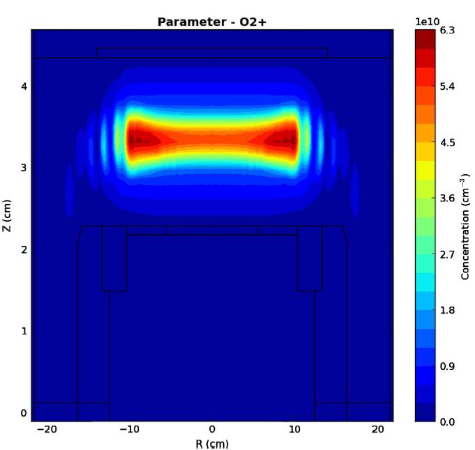
Process-induced variations have a significant impact on the operation of the fabricated devices or interconnect structures. To be able to capture the effect of manufacturing parameters on the resulting structures, equipment simulation is needed. The implementation of this analysis for a PECVD (plasma-enhanced chemical vapor deposition) process is demonstrated which needs treatment of a plasma process on the equipment as well as on the feature scale. The interface between both scales is based on transferring the relevant neutral and ion flux data. This allows one to study the influence of the equipment settings on the structure geometry.
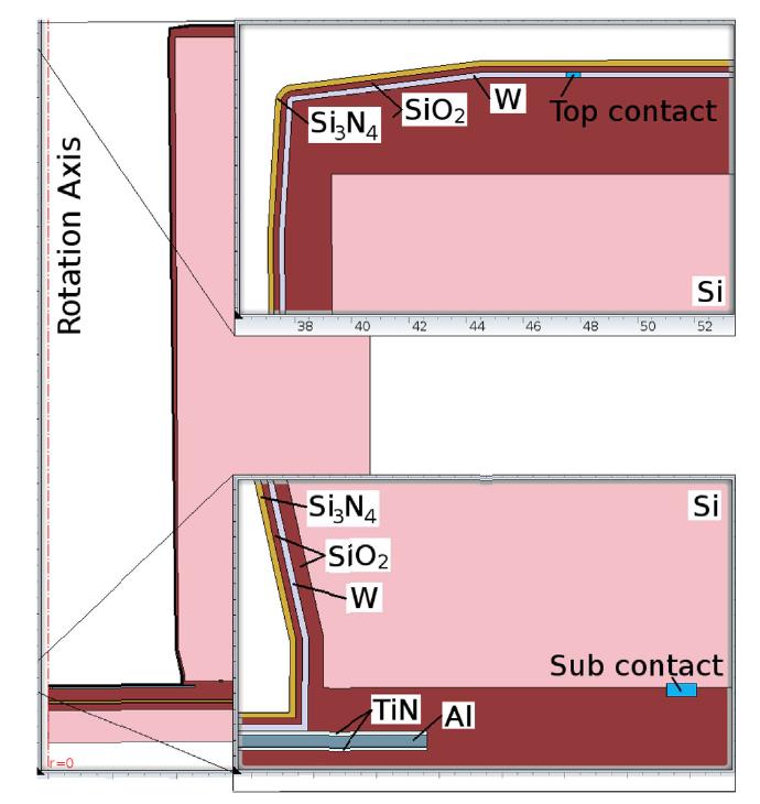
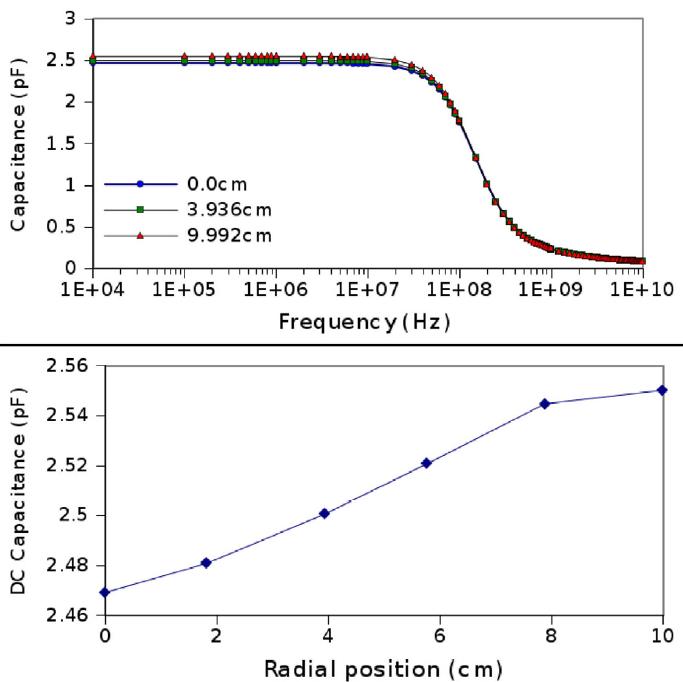
In the example presented, the influence of the feature position is considered. By transferring the structures to a electrical and mechanical finite-element (FEM) simulation tool, the influence of the equipment parameters on quantities such as electrical characteristics or mechanical stress development has been analyzed. The simulations predict an across wafer variation of the parasitic DC capacitance between the tungsten metallization and the silicon substrate of about 3 %. However, mechanical simulations indicate only a minor influence of the oxide layer thickness variation on the reliability performance of the TSV.
References
E. Baer, P. Evanschitzky, J. Lorenz, F. Roger, R. Minixhofer, L. Filipovic, R.L. de Orio, S. Selberherr, Coupled Simulation to Determine the Impact of across Wafer Variations in Oxide PECVD on Electrical and Reliability Parameters of Through-silicon Vias, Microelectronic Engineering 137 (2015) 141
L. Filipovic, R.L. de Orio, S. Selberherr, A. Singulani, F. Roger, R. Minixhofer, Effects of Sidewall Scallops on Open Tungsten TSVs, Proceedings International Relaibility Physics Symposium (IRPS) 2014
L. Filipovic, R.L. de Orio, S. Selberherr, Process and Reliability of SF6/O2 Plasma Etched Copper TSVs, Proceedings EuroSimE 2014
L. Filipovic, F. Rudolf, E. Baer, P. Evanschitzky, J. Lorenz, F. Roger, A. Singulani, R. Minixhofer, S. Selberherr, Three-Dimensional Simulation for the Reliability and Electrical Performance of Through-Silicon Vias, in: Proceedings of Conference on Simulation of Semiconductor Processes and Devices 2014 (SISPAD 2014), p. 341
L. Filipovic, S. Selberherr, The Effects of Etching and Deposition on the Performance and Stress Evolution of Open Through Silicon Vias, Microelectr. Reliab. 54 (2014) 1953