Hierarchical Simulation of Variability
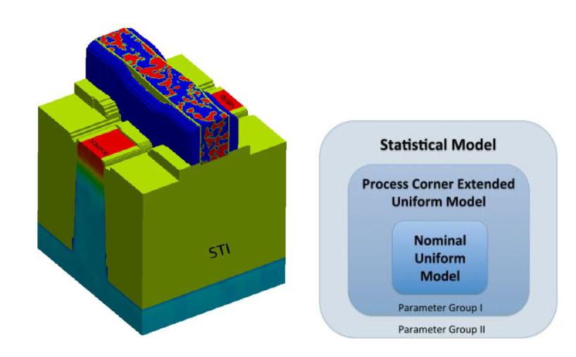
The ever-increasing impact of systematic and stochastic process variations on device and circuit performance requires their accurate and efficient treatment at the circuit and system level. We have employed a novel approach that enables the hierarchical simulation of variability from its sources at the device level to circuit. This is achieved via a process-variability-aware compact modeling methodology which is capable of including the correlations between the effects of sources of variability which occur when different quantities, e.g. the critical dimensions of different transistors, are influenced by process variation.
As a demonstrator of the SUPERTHEME methodology and tool chain, variations in tool level processes such as defocus and threshold in lithography steps are combined with intrinsic sources of variability such as random dopant fluctuations (RDF), line-edge roughness (LER) and metal gate granularity (MGG). As an example, an SRAM cell is studied, consisting of six 20 nm planar bulk transistors, which has been patterned with one Litho-Freeze-Litho-Etch (LFLE) double patterning step and one standard 193 nm lithography step.
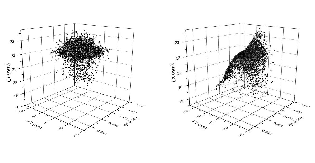
To study the impact of defocus and dose on device behavior, the feature sizes created in optical lithography across a range of values were simulated with the Dr.LiTHO software from IISB providing the distributions of device CD due to process variation as shown in Figure 1. A design of experiments (DoE) matrix consisting of 25 NMOS and 25 PMOS transistors with different gate lengths and gate widths was then transferred to the GSS device simulator GARAND, and the device behaviour over the range of geometries is simulated. Then the impact of RDF, LER and MGG for each node of the DoE matrix is also simulated (as illustrated in Figure 2a). Employing a unified compact modeling strategy (illustrated in Figure 2b) and the GSS compact model extractor MYSTIC compact models are created that capture the impact of both the process and the statistical variability as well as the correlations between them.
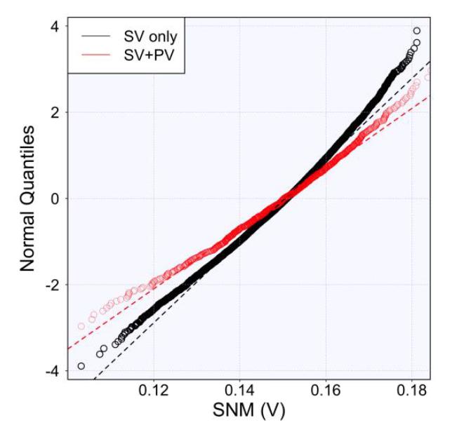
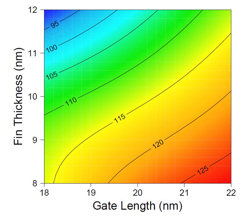
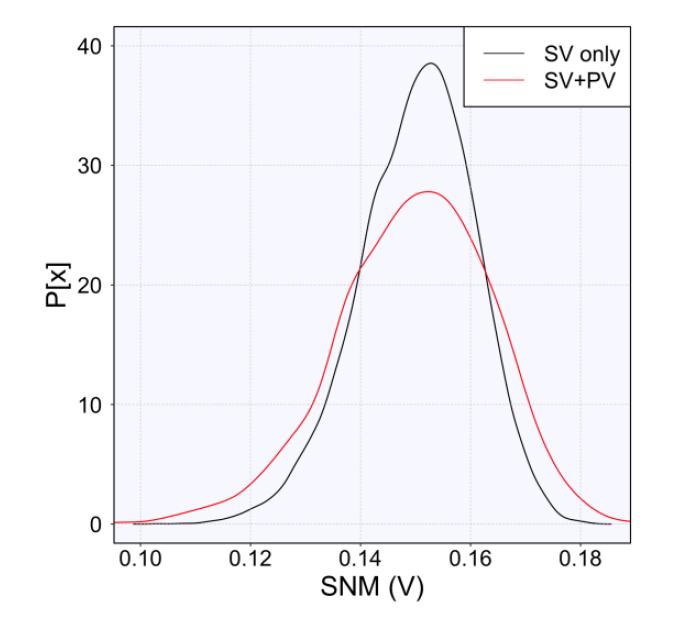
These ‘process-variability-aware’ compact models are then supplied to the GSS statistical circuit simulation engine RandomSpice and simulations of the Static Noise Margin (SNM) of the example 6T SRAM cell were performed. The impact of combined process and statistical variability leads to significant variations in the statistics of SNM across the process space. This approach enables the simultaneous and efficient assessment of the impact of systematic and statistical process variations on devices and circuits, including process-induced correlations. Figures 3 and 4 compare how SNM varies when Monte Carlo process variations are included in the circuit level simulations and Figure 5 illustrates how the -3-sigma SNM is subject to changes in statistical variations across the process space.